Brussels – The European Commission has announced the launch of NanoIC, a European facility for the design of advanced chips, at the Interuniversity Centre for Microelectronics in Leuven, Belgium. With an investment of 2.5 billion euros, including 700 million euros from the EU, the same amount from national and regional governments, and 1.1 billion euros from the Dutch company ASML and other industrial partners, NanoIC’s ultimate goal is to create “enormous opportunities to accelerate innovation in strategic European markets” such as automotive, healthcare and life sciences, industrial automation, network infrastructure and quantum computing.
The facility, located a few kilometres from Brussels, was inaugurated by Vice-President of the Executive and Commissioner for Technological Sovereignty, Security and Democracy, Henna Virkkunen, Belgian Prime Minister Bart De Wever, and Minister-President of Flanders Matthias Diependaele. The NanoIC centre “will accelerate the development of next-generation semiconductor technology, essential for the development of AI, autonomous vehicles, healthcare and 6G mobile technology,” according to a statement released by the European Commission.
Almost two and a half years after the entry into force of the European Chips, which aims to mobilise 43 billion euros in public and private investment by the end of the decade, the Commission is trying to change pace. The investment in the NanoIC facility responds to the urgency highlighted on 25 September by the Semiconductor Coalition, which brings together experts from all member countries: in a joint statement, the 27 member states called for raising the bar and revising the targets of European legislation in a reinforced Chips Act, with the aim “to strengthen Europe’s position in the global semiconductor value chain.” This chain is still dominated by China, the world leader in production, and Taiwan, which is in fact the main supplier to most Western companies.
Specifically, the launch of NanoIC is part of the “Chips for Europe” initiative, which falls under the broader European chip strategy and comprises a series of pilot lines for process development, testing, and small-scale production. These “will serve as a platform for European research and development with an industrial perspective, bridging the gap between the laboratory and the factory,” according to a European Commission press release.
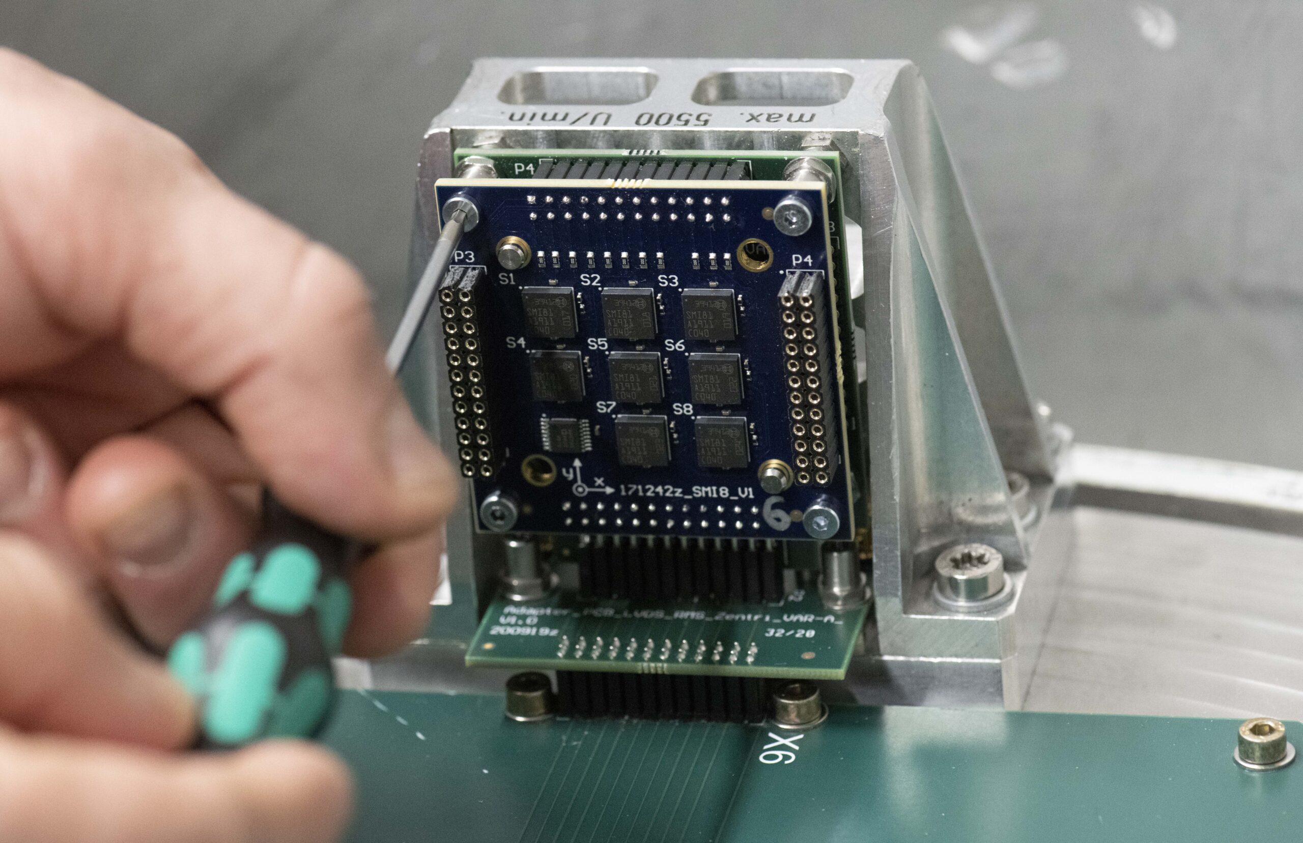
The centre will be the first facility in Europe to implement the most advanced extreme ultraviolet lithography machine, focusing on the design and production of chips using technologies beyond two nanometres, and will enable researchers and companies to test new chip designs, equipment, and processes on a near-industrial scale prior to mass production. The project is based on the open access principle, with start-ups, researchers, small and medium-sized enterprises, and large organisations able to use NanoIC’s facilities.
English version by the Translation Service of Withub